Presentation on the topic: “Semiconductor diodes” Completed by: Barmin R.A. Gelzin I.E. A semiconductor diode is a nonlinear electronic device with two terminals. Depending on the internal structure, type, quantity and level of doping of the internal elements of the diode and the current-voltage characteristics, the properties of semiconductor diodes vary. We will consider the following types of diodes: rectifier diodes based on pn junction, zener diodes, varicaps, tunnel and reverse diodes. J J s (e VG 1) Rectifier diode based on p-n junction The basis of the rectifier diode is an ordinary electron-hole junction; the current-voltage characteristic of such a diode has a pronounced nonlinearity. In forward bias, the diode current is injection, large in magnitude, and represents the diffusion component of the majority carrier current. When reverse biased, the diode current is small in magnitude and represents the drift component of the minority carrier current. In the equilibrium state, the total current due to the diffusion and drift currents of electrons and holes is zero. Rice. Parameters of a semiconductor diode: a) current-voltage characteristic; b) the design of the current-voltage characteristic housing is described by the equation J J s (e VG 1) Rectification in a diode One of the main properties of a semiconductor diode based on a p-n junction is the sharp asymmetry of the current-voltage characteristic: high conductivity with forward bias and low with reverse bias. This diode property is used in rectifier diodes. The figure shows a diagram illustrating the rectification of alternating current in a diode. - Rectification coefficient of an ideal diode based on a p-n junction. Characteristic resistance There are two types of characteristic resistance of diodes: differential resistance rD and direct current resistance RD. Differential resistance is defined as DC resistance RD U I U I 0 (e U 1) In the forward section of the current-voltage characteristic, the DC resistance is greater than the differential resistance RD > rD, and in the reverse section it is less than RD< rD. Стабилитроны Стабилитрон - это полупроводниковый диод, вольт-амперная характеристика которого имеет область резкой зависимости тока от напряжения на обратном участке вольт-амперной характеристики. ВАХ стабилитрона имеет вид, представленный на рисунке При достижении напряжения на стабилитроне, называемого напряжением стабилизации Uстаб, ток через стабилитрон резко возрастает. Дифференциальное сопротивление Rдиф идеального стабилитрона на этом участке ВАХ стремится к 0, в реальных приборах величина Rдиф составляет значение: Rдиф 250 Ом. Основное назначение стабилитрона – стабилизация напряжения на нагрузке, при изменяющемся напряжении во внешней цепи. В связи с этим последовательно со стабилитроном включают нагрузочное сопротивление, демпфирующее изменение внешнего напряжения. Поэтому стабилитрон называют также опорным диодом. Напряжение стабилизации Uстаб зависит от физического механизма, обуславливающего резкую зависимость тока от напряжения. Различают два физических механизма, ответственных за такую зависимость тока от напряжения, – лавинный и туннельный пробой p-n перехода. Для стабилитронов с туннельным механизмом пробоя напряжение стабилизации Uстаб невелико и составляет величину менее 5 вольт: Uстаб < 5 В. Для стабилитронов с лавинным механизмом пробоя напряжение стабилизации обычно имеет большие значения и составляет величину более 8 вольт: Uстаб > 8 V. Varicaps Varicap is a semiconductor diode, the operation of which is based on the dependence of the barrier capacitance of the p-n junction on the reverse voltage. Varicaps are used as elements with electrically controlled capacitance in circuits for tuning the frequency of an oscillatory circuit, dividing and multiplying frequencies, frequency modulation, controlled phase shifters, etc. In the absence of external voltage, a potential barrier and an internal electric field exist in the p-n junction. If reverse voltage is applied to the diode, the height of this potential barrier will increase. An external reverse voltage pushes electrons deeper into the region, resulting in an expansion of the depleted region of the pn junction, which can be thought of as a simple flat capacitor in which the plates are the boundaries of the region. In this case, in accordance with the formula for the capacitance of a flat capacitor, with increasing distance between the plates (caused by an increase in the reverse voltage value), the capacitance of the p-n junction will decrease. This reduction is limited only by the thickness of the base, beyond which the transition cannot expand. Once this minimum is reached, the capacitance does not change with increasing reverse voltage. A tunnel diode is a semiconductor diode based on a p+-n+ junction with heavily doped regions, in the forward section of the current-voltage characteristic of which an n-shaped dependence of current on voltage is observed. In an n+-type semiconductor, all states in the conduction band up to the Fermi level are occupied by electrons, and in a p+-type semiconductor, by holes. Band diagram of a p+-n+ junction formed by two degenerate semiconductors: Let's calculate the geometric width of the degenerate p-n junction. We will assume that in this case the asymmetry of the p-n junction is preserved (p+ is a more heavily doped region). Then the width of the p+-n+ transition is small: 2 s 0 2 0 W 2 s 0 E g qN D 2 1 10 qN D 12 1.6 10 19 1 6 ~ 10 см ~ 100 Å Let us estimate the de Broglie wavelength of the electron from simple relations: E 2 2 2 2m 2 kT ; 2 mkT h 2 1 h 2 mkT 2 9.1 10 31 1. 38 10 6. 3 10 34 23 300 ~ 140 Å Thus, the geometric width of the p+-n+ transition turns out to be comparable to the de Broglie wavelength of the electron. In this case, in a degenerate p+-n+ junction one can expect the manifestation of quantum mechanical effects, one of which is tunneling through a potential barrier. With a narrow barrier, the probability of tunneling seepage through the barrier is nonzero. A reverse diode is a tunnel diode without a negative differential resistance section. The high nonlinearity of the current-voltage characteristic at low voltages near zero (on the order of microvolts) allows this diode to be used for detecting weak signals in the microwave range. Current-voltage characteristic of a germanium reverse diode a) total current-voltage characteristic; b) reverse section of the current-voltage characteristic at different temperatures
zener diode
7
Voltage stabilizer based on a zener diode and current-voltage characteristics of zener diodes 1-KS133A, 2-KS156A, 3-KS182Zh, 4-KS212Zh
Voltage stabilizer basedzener diode and current-voltage characteristics of zener diodes 1-KS133A, 2KS156A, 3-KS182Zh, 4-KS212Zh
Stepanov Konstantin Sergeevich Current-voltage characteristics
1-KS133A, 2-KS156A, 3-KS182Zh, 4-KS212Zh
9
Stepanov Konstantin Sergeevich Varicap: designation and its wach
Maximum varicap capacity
is 5-300 pF
10
Stepanov Konstantin Sergeevich Stepanov Konstantin Sergeevich
APPLICATION OF DIODES
In electrical engineering:1) rectifier devices,
2) protective devices.
Stepanov Konstantin Sergeevich
RECTIFIER DIAGRAMS
Stepanov Konstantin SergeevichStepanov Konstantin Sergeevich
Operation of a half-wave rectifier
Rectifier output voltageu(t) = u(t) - u(t),
As an average value -
U = Um/π,
heat
entrance
heat
Stepanov Konstantin Sergeevich
diode
RECTIFIER DIAGRAMS
Single Phase Full Wave Rectifierwith midpoint
Stepanov Konstantin Sergeevich
Single Phase Full Wave Rectifier with Mid Point
Stepanov Konstantin SergeevichFull-wave rectifier operation
also determined by the second law
Kirchhoff:
As an instantaneous value -
u (t)= u (t) - u (t),
In the form of effective value –
U = 2Um/π
heat
entrance
heat
Stepanov Konstantin Sergeevich
diode
RECTIFIER DIAGRAMS
Stepanov Konstantin SergeevichSingle phase bridge rectifier
Stepanov Konstantin SergeevichOperation of a full-wave bridge rectifier
In this circuit, the output voltagedetermined by Kirchhoff's second law:
As an instantaneous value -
u (t)= u (t) - 2u (t),
In the form of effective value –
U = 2Um/π,
while ignoring the voltage drop across
diodes due to their small size.
heat
entrance
heat
Stepanov Konstantin Sergeevich
diode
RECTIFIER DIAGRAMS
Stepanov Konstantin Sergeevich Ripple frequencyf1п = 3 fс
Stepanov Konstantin Sergeevich
RECTIFIER DIAGRAMS
Stepanov Konstantin SergeevichThree-phase bridge control circuit
The constant component in this circuitbig enough
m
, then Ud 0 =0.955Uл m,
U 2 U Sin
d0
2
m
where: U2 – effective value of the linear
rectifier input voltage,
m – number of rectifier phases.
Ul m - amplitude value of linear
voltage
The amplitudes of harmonic pulsations are small,
and their pulsation frequency is high
Um1 = 0.055Uл m (frequency f1п = 6 fс)
Um2 = 0.013Uл m (frequency f2п = 12 fс)
Stepanov Konstantin Sergeevich
NETWORK FILTERS
Capacitive (C – filters)Inductive (L – filters)
LC - filters
Stepanov Konstantin Sergeevich
Capacitive (C – filter)
Stepanov Konstantin SergeevichCapacitive (C – filter)
Stepanov Konstantin SergeevichCapacitive (C – filter)
Stepanov Konstantin SergeevichInductive (L – filter)
Stepanov Konstantin SergeevichInductive (L – filter)
Stepanov Konstantin Sergeevich Stepanov Konstantin Sergeevich Bipolar transistorsBipolar transistor
called semiconductor
device with two p-n junctions.
It has a three-layer structure
n-p-n or p-n-p-type
33
Stepanov Konstantin Sergeevich Structure and notation
bipolar transistor
34
Stepanov Konstantin Sergeevich
Stepanov Konstantin Sergeevich
Bipolar transistor structure
Stepanov Konstantin Sergeevich Transistor operating modesThe following transistor modes are distinguished:
1) current cut-off mode (closed mode
transistor) when both junctions are biased
reverse direction (closed); 2)mode
saturation (open transistor mode),
when both transitions are forward biased
direction, the currents in the transistors are maximum and
do not depend on its parameters: 3) active mode,
when the emitter junction is forward biased
direction, collector - in the opposite direction.
37
Stepanov Konstantin Sergeevich
Scheme with a common base
Stepanov Konstantin Sergeevich Circuit with a common base and its current-voltage characteristic39
Stepanov Konstantin Sergeevich
Common emitter (CE) circuit
Stepanov Konstantin SergeevichCircuit with a common collector (OK)
Stepanov Konstantin SergeevichCircuit with OE(a), its current-voltage characteristic and circuit with OK(b)
Stepanov Konstantin SergeevichCharacteristics and equivalent circuits of transistors
Stepanov Konstantin SergeevichCommon emitter circuit
Stepanov Konstantin SergeevichOscillograms at the input and output of an amplifier with OE
Stepanov Konstantin SergeevichCommon emitter circuit
Stepanov Konstantin Sergeevich Stepanov Konstantin SergeevichThyristors
Multilayer structures with three p-n junctions are called thyristors.Thyristors with two terminals
(two-electrode) are called
dinistors,
with three (three-electrode) -
thyristors.
Stepanov Konstantin Sergeevich
Thyristor properties
The main property isability to be in two
states of stable equilibrium:
as open as possible, and
as closed as possible.
Stepanov Konstantin Sergeevich
Thyristor properties
You can turn on thyristorslow power pulses along the circuit
management.
Turn off - change polarity
power circuit voltage or
decreasing the anode current to
values below the holding current.
Stepanov Konstantin Sergeevich
Application of thyristors
For this reason, thyristors are classified asswitching class
semiconductor devices, mainly
the application of which is
contactless switching
electrical circuits.
Stepanov Konstantin Sergeevich
Structure, designation and current-voltage characteristics of the dinistor.
Stepanov Konstantin Sergeevich When the dinistor is turned on directly, the sourcepower supply En biases p-n junctions P1 and P3 to
forward direction, and P2 - in the opposite direction,
the dinistor is in the closed state and
all voltage applied to it drops
at transition P2. The device current is determined
leakage current Iut, the value of which
is in the range of hundredths
microampere to several microampere
(section OA). Differential
u
dinistor resistance Rdiff = l in the section
OA is positive and quite large. His
the value can reach several hundred
megaohm On the AB section Rdiff<0 Условное
The dinistor designation is shown in Fig.b.
Stepanov Konstantin Sergeevich
Thyristor structure
Stepanov Konstantin SergeevichThyristor designation
Stepanov Konstantin Sergeevich Stepanov Konstantin Sergeevich Stepanov Konstantin Sergeevich Stepanov Konstantin SergeevichConditions for turning on the thyristor
1. Forward voltage on the thyristor(anode +, cathode -).
2. Control pulse opening
thyristor should be sufficient
power.
3. Load resistance should
be less than critical
(Rcr = Umax/Isp).
Stepanov Konstantin Sergeevich Field effect transistors
60
Stepanov Konstantin Sergeevich
Field-effect (unipolar) transistors
Stepanov Konstantin SergeevichInsulated gate field effect transistor
Stepanov Konstantin SergeevichFEEDBACK Prepared by Stepanov K.S.
Stepanov Konstantin SergeevichFEEDBACK
The influence of cause on effect,causing this cause is called
feedback.
Feedback that reinforces
positive (POS).
Feedback weakening
the effect of the consequence is called
negative (NOS).
Stepanov Konstantin Sergeevich
FEEDBACK OS block diagram
Stepanov Konstantin SergeevichSerial current feedback
Stepanov Konstantin SergeevichSerial current feedback
Amplifier gain inU out
direction of the arrow
K
U in
Reverse transmission coefficient
connections in the direction of the arrow
U os
U out
Stepanov Konstantin Sergeevich
Serial current feedback
β shows what part of the outputvoltage is transmitted to the input.
Usually
1
U in U in U oc U in U out
U out KU in K (U in U out)
Stepanov Konstantin Sergeevich
Serial current feedback
HenceThen
K
K
1 K
U out
K
K KK
U in
U os
U out Z n
K
1
Zн
K
1 K
Stepanov Konstantin Sergeevich
Serial current feedback
Input impedanceSince in the scheme
Then
Z in (1 K) Z in
U os (I out I in)
U in U in (I out I in)
Z in Z in (1 K I)
Z out (1 K in)
Z out
Stepanov Konstantin Sergeevich
Serial current feedback
Where KI is the current amplification factor. Hemust be less than zero, i.e. amplifier
must be inverting.
K in Zin * Kin /(Rg Zin)
At OOS K in<0
Used when you need to have
large Zout. Then such an amplifier
equivalent to a current generator. At
deep OOS is fair
>>Zout
Z out
Stepanov Konstantin Sergeevich
Stepanov Konstantin Sergeevich
Serial voltage feedback
Serial OSvoltage
By
Increases input and decreases
output impedance
Z out
Z out
1 K in
Z in
Rg Z in
where Kv – transmission coefficient
amplifier in idle mode
Emitter Follower – Bright
example of Sequential OOS
voltage
Stepanov Konstantin Sergeevich
Parallel current feedback
ParallelStepanov Konstantin Sergeevich
OOS by current
Parallel voltage feedback
Stepanov Konstantin SergeevichLOGICAL ELEMENTS Prepared by Stepanov K.S.
Stepanov Konstantin SergeevichLOGIC ELEMENTS
Logic elements - devices,intended for processing
information in digital form
(sequences of signals high -
"1" and low - "0" levels in binary
logic, the sequence "0", "1" and "2" in
ternary logic, sequence "0",
"1", "2", "3", "4", "5", "6", "7", "8" and "9" in
Stepanov Konstantin Sergeevich
LOGIC ELEMENTS
Physically, logical elementscan be fulfilled
mechanical,
electromechanical (on
electromagnetic relays),
electronic (on diodes and
transistors), pneumatic,
hydraulic, optical, etc.
Stepanov Konstantin Sergeevich
LOGIC ELEMENTS
After the proof of the theorem in 1946John von Neumann on economy
exponential positional systems
reckoning became known about
advantages of binary and ternary
number systems compared to
decimal number system.
Stepanov Konstantin Sergeevich
LOGIC ELEMENTS
Duality and trinity allowssignificantly reduce the number
operations and elements performing
this treatment, compared to
decimal logic gates.
Logic elements perform
logical function (operation) with
input signals (operands,
data).
Stepanov Konstantin Sergeevich
LOGIC ELEMENTS
Logical operations with oneoperand are called unary, with
two - binary, with three -
ternary (triary,
trinary), etc.
Stepanov Konstantin Sergeevich
LOGIC ELEMENTS
Of the possible unary operations withunary output is of interest to
implementations represent operations
negations and repetitions, moreover,
the negation operation has a large
significance than the repetition operation, Stepanov Konstantin SergeevichA Mnemonic rule For equivalence with any
The output will be:
an even number of “1” is valid,
an odd number of “1s” is valid,
Stepanov Konstantin Sergeevich
Addition modulo 2 (2XOR, unequal). Inversion of equivalence.
AStepanov Konstantin Sergeevich
0
0
1
1
B
0
1
0
1
f(AB)
0
1
1
0
Mnemonic rule
For a sum modulo 2 with anynumber of inputs sounds like this:
The output will be:
"1" if and only if at the input
an odd number of “1s” is valid,
"0" if and only if at the input
an even number of “1” is valid,
Stepanov Konstantin Sergeevich Thank you for attention
Stepanov Konstantin Sergeevich


1 of 9
Presentation on the topic: semiconductor devices
Slide no. 1

Slide description:
Slide no. 2

Slide description:
The rapid development and expansion of the areas of application of electronic devices is due to the improvement of the element base, the basis of which is semiconductor devices. Semiconductor materials in their resistivity (ρ = 10-6 ÷ 1010 Ohm m) occupy an intermediate place between conductors and dielectrics. The rapid development and expansion of the areas of application of electronic devices is due to the improvement of the element base, the basis of which is semiconductor devices. Semiconductor materials in their resistivity (ρ = 10-6 ÷ 1010 Ohm m) occupy an intermediate place between conductors and dielectrics.
Slide no. 3

Slide description:
Slide no. 4

Slide description:
For the manufacture of electronic devices, solid semiconductors with a crystalline structure are used. For the manufacture of electronic devices, solid semiconductors with a crystalline structure are used. Semiconductor devices are devices whose operation is based on the use of the properties of semiconductor materials.
Slide no. 5
Slide description:
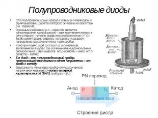
Semiconductor diodes This is a semiconductor device with one p-n junction and two terminals, the operation of which is based on the properties of the p-n junction. The main property of a p-n junction is one-way conductivity - current flows only in one direction. The conventional graphic designation (UGO) of the diode has the shape of an arrow, which indicates the direction of current flow through the device. Structurally, the diode consists of a p-n junction enclosed in a housing (with the exception of micromodular unpackaged ones) and two terminals: from the p-region - the anode, from the n-region - the cathode. Those. A diode is a semiconductor device that passes current in only one direction - from the anode to the cathode. The dependence of the current through the device on the applied voltage is called the current-voltage characteristic (volt-ampere characteristic) of the device I=f(U).
Slide no. 6
Slide description:
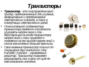
Transistors A transistor is a semiconductor device designed to amplify, generate and convert electrical signals, as well as switch electrical circuits. A distinctive feature of the transistor is the ability to amplify voltage and current - the voltages and currents acting at the input of the transistor lead to the appearance of significantly higher voltages and currents at its output. The transistor got its name from the abbreviation of two English words tran(sfer) (re)sistor - controlled resistor. The transistor allows you to regulate the current in the circuit from zero to the maximum value.
Slide no. 7

Slide description:
Classification of transistors: Classification of transistors: - according to the principle of operation: field-effect (unipolar), bipolar, combined. - according to the value of power dissipation: low, medium and high. - according to the limiting frequency value: low-, medium-, high- and ultra-high-frequency. - according to the operating voltage: low- and high-voltage. - by functional purpose: universal, amplifier, key, etc. - by design: unframed and cased, with rigid and flexible leads.
Slide no. 8

Slide description:
Depending on the functions performed, transistors can operate in three modes: Depending on the functions performed, transistors can operate in three modes: 1) Active mode - used to amplify electrical signals in analog devices. The resistance of the transistor changes from zero to the maximum value - they say the transistor “opens slightly” or “closes slightly”. 2) Saturation mode - the transistor resistance tends to zero. In this case, the transistor is equivalent to a closed relay contact. 3) Cut-off mode - the transistor is closed and has a high resistance, i.e. it is equivalent to an open relay contact. Saturation and cutoff modes are used in digital, pulse and switching circuits.
Slide no. 9

Slide description:
Indicator An electronic indicator is an electronic indicating device designed for visual monitoring of events, processes and signals. Electronic indicators are installed in various household and industrial equipment to inform a person about the level or value of various parameters, for example, voltage, current, temperature, battery charge, etc. An electronic indicator is often mistakenly called a mechanical indicator with an electronic scale.
Slide 1

Slide 2
Conductors, dielectrics and semiconductors. Intrinsic (electron-hole) electrical conductivity. Impurity (electron-hole) electrical conductivity. Electron-hole transition. Contact of two semiconductors with p- and n-conductivity. P-n junction and its properties. Structure of a semiconductor diode. Volt - ampere characteristic of a semiconductor diode. * * * * Application of semiconductors (alternating current rectification)*. Full-wave AC rectification.* Full-wave AC rectification.* LEDs*.

Slide 3
This version of the presentation includes 25 slides out of 40, some of which are limited to view. The presentation is for demonstration purposes only. The full version of the presentation contains almost all the material on the topic “Semiconductors,” as well as additional material that should be studied in more detail in a specialized physics and mathematics class. The full version of the presentation can be downloaded from the author’s website LSLSm.narod.ru.

Slide 4
Non-conductors (dielectrics)
Conductors
First of all, let us explain the concept itself - a semiconductor.
Based on their ability to conduct electrical charges, substances are conventionally divided into conductors and non-conductors of electricity.
Bodies and substances in which electric current can be created are called conductors.
Bodies and substances in which electric current cannot be created are called non-conductors of current.
Metals, coal, acids, salt solutions, alkalis, living organisms and many other bodies and substances.
Air, glass, paraffin, mica, varnish, porcelain, rubber, plastics, various resins, oily liquids, dry wood, dry fabric, paper and other substances.
Semiconductors in electrical conductivity occupy an intermediate position between conductors and non-conductors.

Slide 5
Boron B, carbon C, silicon Si phosphorus P, sulfur S, germanium Ge, arsenic As, selenium Se, tin Sn, antimony Sb, tellurium Te and iodine I.
Semiconductors are a number of elements of the periodic table, most minerals, various oxides, sulfides, tellurides and other chemical compounds.

Slide 6
An atom consists of a positively charged nucleus and negatively charged electrons rotating around the nucleus in stable orbits.
The electron shell of a germanium atom consists of 32 electrons, four of which rotate in its outer orbit.
Electron shell of an atom
Atomic nucleus
How many electrons does a germanium atom have?
The four outer electrons, called valence electrons, essentially define the germanium atom. The germanium atom strives to acquire a stable structure inherent in atoms of inert gases and characterized by the fact that in their outer orbit there is always a strictly defined number of electrons (for example, 2, 8, 18, etc.). Thus, in order to acquire such a structure, the germanium atom it would be necessary to accept four more electrons into the outer orbit.

Slide 7

Slide 8
As the temperature increases, some of the valence electrons may gain enough energy to break covalent bonds. Then free electrons (conduction electrons) will appear in the crystal. At the same time, vacancies are formed in places where bonds are broken, which are not occupied by electrons. These vacancies are called holes.
ρmet = f(T) ρsemi = f(T)
Let's increase the temperature of the semiconductor.
Valence electrons in a germanium crystal are much more strongly bound to atoms than in metals; Therefore, the concentration of conduction electrons at room temperature in semiconductors is many orders of magnitude lower than in metals. Near absolute zero temperature in a germanium crystal, all electrons are occupied in the formation of bonds. Such a crystal does not conduct electric current.
As the temperature of a semiconductor increases, a larger number of electron-hole pairs are formed per unit time.
Dependence of metal resistivity ρ on absolute temperature T
Intrinsic electrical conductivity

Slide 9
The electron-hole conductivity mechanism manifests itself only in pure (i.e., without impurities) semiconductors and is therefore called intrinsic electrical conductivity.
Impurity (electron-hole) electrical conductivity.
The conductivity of semiconductors in the presence of impurities is called impurity conductivity.
Impurity (electronic) electrical conductivity.
Impurity (hole) electrical conductivity.
By changing the concentration of impurities, you can significantly increase the number of charge carriers of one sign or another and create semiconductors with a predominant concentration of either negatively or positively charged carriers.
Impurity centers can be: atoms or ions of chemical elements embedded in the semiconductor lattice; excess atoms or ions embedded in lattice interstices; various other defects and distortions in the crystal lattice: empty nodes, cracks, shifts that occur during deformation of crystals, etc.

Slide 10
Electronic conductivity occurs when pentavalent atoms (for example, arsenic, As) are introduced into a germanium crystal with tetravalent atoms.
Further content of the slide is in the full version of the presentation.

Slide 11

Slide 12


Slide 14

Slide 15

Slide 16
The ability of an n-p junction to pass current in almost only one direction is used in devices called semiconductor diodes. Semiconductor diodes are made from silicon or germanium crystals. During their manufacture, an impurity is fused into a crystal with a certain type of conductivity, providing a different type of conductivity.
Semiconductor diodes are depicted on electrical circuits in the form of a triangle and a segment drawn through one of its vertices parallel to the opposite side. Depending on the purpose of the diode, its designation may contain additional symbols. In any case, the sharp point of the triangle indicates the direction of forward current flow through the diode. The triangle corresponds to the p-region and is sometimes called the anode, or emitter, and the straight segment corresponds to the n-region and is called the cathode, or base.
Base B Emitter E

Slide 17

Slide 18
By design, semiconductor diodes can be planar or point.
As a rule, diodes are made of germanium or silicon crystal, with n-type conductivity. A drop of indium is melted into one of the surfaces of the crystal. Due to the diffusion of indium atoms deep into the second crystal, a p-type region is formed in it. The rest of the crystal still has n-type conductivity. A p-n junction occurs between them. To prevent exposure to moisture and light, as well as for strength, the crystal is enclosed in a housing and provided with contacts. Germanium and silicon diodes can operate in different temperature ranges and with currents of different strengths and voltages.
Diode rectifiers Larionov A. N. three-phase rectifier on three half-bridges Diodes are widely used to convert alternating current into direct current (more precisely, into unidirectional pulsating current). A diode rectifier or diode bridge (that is, 4 diodes for a single-phase circuit (6 for a three-phase half-bridge circuit or 12 for a three-phase full-bridge circuit), interconnected in a circuit) is the main component of power supplies for almost all electronic devices. A three-phase diode rectifier according to A. N. Larionov’s circuit on three parallel half-bridges is used in automobile generators; it converts the alternating three-phase current of the generator into direct current of the vehicle’s on-board network. The use of an alternating current generator in combination with a diode rectifier instead of a direct current generator with a brush-commutator assembly has made it possible to significantly reduce the size of a car alternator and increase its reliability. Some rectifier devices still use selenium rectifiers. This is due to the peculiarity of these rectifiers that when the maximum permissible current is exceeded, selenium burns out (in sections), which does not lead (to a certain extent) to either a loss of rectifying properties or a short circuit - breakdown. High-voltage rectifiers use selenium high-voltage columns from a plurality of series-connected selenium rectifiers and silicon high-voltage columns from a plurality of series-connected silicon diodes. Diode Detectors Diodes, in combination with capacitors, are used to isolate low-frequency modulation from amplitude-modulated radio signals or other modulated signals. Diode detectors are used in almost all [source not specified 180 days] radio receiving devices: radios, televisions, etc. The quadratic portion of the current-voltage characteristic of the diode is used. Diode protection Diodes are also used to protect various devices from incorrect switching polarity, etc. There is a well-known diode protection scheme for DC circuits with inductances from surges when the power is turned off. The diode is connected in parallel with the coil so that in the “operating” state the diode is closed. In this case, if you abruptly turn off the assembly, a current will arise through the diode and the current strength will decrease slowly (the induced emf will be equal to the voltage drop across the diode), and there will not be a powerful voltage surge leading to sparking contacts and burnt-out semiconductors. Diode switches Are used for switching high-frequency signals. The control is carried out by direct current, the RF and control signal are separated using capacitors and inductors. Diode spark protection This does not exhaust the use of diodes in electronics, but other circuits, as a rule, are very highly specialized. Special diodes have a completely different area of applicability, so they will be discussed in separate articles.


Celebration of Knowledge Day in children's library N3
UIS in the field of procurement: what is it, what is it intended for?
Forecasting using Excel (Excel models examples methods)
Theater ticket distribution
Release of working capital Working capital release ratio formula